

This is an intro to the FPD-Link display interface, commonly used in laptop and monitor LCD panels. Information surrounding the exact nature of this interface is scattered all over the internet, so I wrote this article to try and make it easier to understand, and potentially useable in your own projects!
FPD-Link is also known as simply “LVDS”, although this is technically incorrect since this refers to just the electrical interface, and LVDS is used for many other interfaces too. The actual interface is called FPD-Link (or also FlatLink by some manufacturers), and describes a general interface for connecting LCD panels to graphics controllers, much like VGA or DVI. However it doesn’t describe an exact data format, so many different options exist for different panels, making it not quite as inter-operable as VGA or DVI.
Fortunately you’ll find most (old) laptop LCD panels will use a de-facto format, so it’s actually not too hard to re-use the screens out of that old stack of laptops you have in the basement!
You can’t juts connect FPD-Link to a computer however, so if you want to use an FPD-Link capable panel you’ll need one of the following:
- An LVDS->HDMI/DVI converter (either a monitor-style one from eBay/Aliexpress, or one that simply converts the signals)
- A board with native LVDS support (Some embedded ARM boards have native LVDS!)
The other thing you will need is a datasheet for your LCD panel, or good reverse-engineering skills!
The rest of this article details the FPD-Link/LVDS interface, and other related things like EDID and converter boards.
Outline
- The FPD-Link Interface - Everything you need to know about driving LVDS LCDs
- Other Interfaces
- Extended Display Identification Data (EDID)
- Reverse engineering - How to reverse engineer your own LCD panel
- Interfacing - How to use your panel in an embedded project
FPD-Link
Flat Panel Display Link (FPD-Link) was created by National Semiconductor as a free and open standard for connecting the output of a GPU or video processor to an LCD panel’s timing controller. It superseeds TTL/CMOS parallel interfaces which were very limited in the resolution they could achieve1. Although FPD-Link itself is becoming outdated with the rise of next generation LCD monitors (2440p and 4K!), it is still used in most current generation laptops and desktop monitors. You can read more about the FPD-Link standard in Texas Instruments’ app-note2.
The protocol itself is fairly straight-forward; there’s no complex control/configuration/packetization of the video data, and usually a panel will accept any resolution given to it since it relies on horizontal and vertical synchronization signals like most other video interfaces (See the Synchronization & Timing Section for how this works).
LVDS
") Figure 1. LVDS (Wikipedia)
Figure 1. LVDS (Wikipedia)At it’s core, FPD-Link uses a number of [Low-Voltage Differential Signalling]3 (LVDS) pairs in order to transfer video data over a high speed link, which is then de-serialized in the LCD panel and used to drive the display. Even though it has less wires than a parallel interface, it allows for much higher speeds due to increased noise tolerance and capabilities of the LVDS pairs (much like how SATA proivdes faster speeds for hard disks than IDE/PATA).
Each LVDS pair consists of two wires: positive and negative, plus a ground shield/reference. This allows the wires to travel much longer distances since the pair is immune to interference and has reduced cross-talk between pairs.
LVDS pairs are quite easy to locate on a PCB, because they are almost always routed as close together as possible, and sometimes have sqiuggly patterns to match the lengths. Keep in mind that the polarity of the LVDS pair is important!
NOTE: Because the LVDS signals are very sensitive and operate at very high speeds, you should be careful when modifying LVDS wiring. You should use twisted pair wire with each pair individually shielded, and you should ensure the lengths of the wires are matched. If you’re not careful, you may introduce too much skew into the data over long distances, causing some bits to arrive later than other bits, corrupting the image!
Data Serialization
The video data sent to the display consists of raw RGB pixels, plus synchronization and control signals (HSYNC, VSYNC, and DE). This is the same as other video interfaces such as TTL Parallel, VGA, DVI, etc.
") Figure 2. FPD Link Serializer (Wikipedia)
Figure 2. FPD Link Serializer (Wikipedia)FPD-Link serializes this data into channels containing 7 bits of data per clock cycle, as shown in Figure 2. For a typical video interface with 18 bits per pixel (bpp), there are 21 bits of data per clock serialized into a total of 4 LVDS channels (3 data + 1 clock, or “3D+1C”). There are of course many other configurations possible depending on the number of links and data bits. For example, a dual-link 24 bpp interface (common in desktop monitors) would use 2x 4 LVDS data channels + 2 LVDS clock channels, or “8D+2C”. Looking at the pairs of wires on the LCD’s circuit board can provide a very good hint as to which format it uses!
The actual layout of bits in this serial stream varies depending on how the manufacturer has decided to implement it, and is described in the Data Framing section below. For 18 bpp displays there is only one specfic format used, but FPD-Link itself is not limited to just 18 bpp video.
FPD-Link has a maximum bandwidth of somewhere around 130Mpps (Mega pixels per second)4 depending on the transceiver, while the LVDS channels operate at 7x this rate. This limits the maximum allowable resolution to about 1280x800@60Hz. It is usually not possible to drive a 1920x1080p display at 60Hz with just one FPD-Link channel, so two channels are doubled up to support higher resolutions. Some extra high resolution monitors may even use up to 4 FPDLink channels, or eDP (embedded Display Port, a completely different protocol) to further increase the bandwidth.
Data Framing
Most old laptop LCDs will likely be 18 bits per pixel (6 bits per colour), and thus use 3 LVDS data pairs and 1 LVDS clock pair (3D+1C). A total of 21 bits are serialized, and the layout inside the LVDS stream is shown in the following timing diagram:5 6
") 18bpp Format (Most Common)
18bpp Format (Most Common)Some panels will support 24 bpp (8 bits per colour), which uses a fourth LVDS data pair (4D+1C) to increase the bit depth while keeping the bandwidth the same. Unfortunately there are two different standards for how the data is serialized for 24 bpp panels! The difference is which bits the fourth data channel (Y3) contains, and it may either contian the least significant bits (LSB) or most significant bits (MSB) of the pixel. According to Texas Instruments, most 24 bit panels assume the MSB is in the 4th channel4, although contradicting info says that 24 bit LSB panels are the most common5. So if in doubt, check your datasheet! The two different formats are shown in the following timing diagrams:5 6
 24bpp LSB Format
 24bpp MSB Format
Note that an 18 bpp panel can be driven by a 24 bpp LSB transmitter by simply omitting the 4th channel (Y3), in which case the lower bits are discarded and it acts as if it was transmitting 6 bits per colour. You cannot drive an 18 bpp panel from a 24 bpp MSB transmitter!5
Some transceivers may even support 30 bit RGB data7, which use an additional channel (5 LVDS data channels in total). I’m unsure on the exact format of this data as I don’t have any 30 bit LCD panels.
Dual Channel
Dual-channel FPD-Link uses a second FPD-Link, sending even pixels on one and odd pixels on the other in order to double the effective bandwidth, thus supporting higher resolutions (eg. 1920x1080@60Hz). Usually two identical clocks are sent for both FPD-Links (8D+2C). Again, this can be 18 or 24 bpp (or higher). According to Texas Instruments there is only one de-facto mapping for dual-channel 24 bit mode6 (MSB Format):
") 24bpp Dual Channel (8D+2C)
24bpp Dual Channel (8D+2C)Note that there are two sets of CLK/VSYNC/HSYNC/DE lines, but these are probably the same signals.
Synchronization & Timing
The data framing format is only half the story when interfacing with an FPD-Link display; the synchronization and timing are also important to ensure the pixels the panel receives actually match the physical panel! This is done through the HSYNC, VYSNC, and DE synchronization signals. It’s not immediately obvious, but not all pixels transmitted are actually displayed - some end up in the so called “blank-time” interval. This is a leftover artifact from the days of CRT monitors when the electron beam actually needed time to move between rows and frames!8 For backwards compatibility the blank-time is still present in DVI & VGA outputs, which is sad because it’s not required at all in digital panels!
The DE (Data Enable) signal marks active pixels, so whenever DE is low it is blanking. The HSYNC signal is toggled at the start of every row, while the VSYNC is toggled at the start of every frame9. Pixels are scanned left-to-right, top-to-bottom.
The following is a generic timing diagram that shows how these signals relate to one another:
 Figure 3. Generic Timing Diagram
NOTE: CLK is the pixel clock, not the LVDS clock!
If you have a datasheet for your LCD panel, it will usually include a timing diagram specifying the values you should use to display a valid picture. This information is also reflected in the panel’s EDID (if present). Generally this information can be represented in the form of a Coordinated Video Timing (CVT), a VESA standard specifying common timing formats for different resolutions10.
The actual format of the pixel data depends on the protocol and wiring. For FPD-Link the pixels are serialized into the format specified in the previous section .
Other Interfaces
Digital Visual Interface (DVI)

Digital Visual Interface (DVI) is actually very similar to FPDLink, in that it uses the exact same data framing format (RGB pixel data + HSYNC/VSYNC/DE). However it uses Transition-Minimized Differential Signalling (TMDS) not LVDS, so it is not electrically compatible11. The digital encoding of data is also different, as it uses a special encoding algorithm to convert the 11 bit inputs to 10 bit codes. The DVI video stream is always 24 bpp, and contains various control signals including HSYNC, VSYNC, and ENABLE (DE)12. This makes it fully compatible with FPD Link, with an appropriate converter chip!
Embedded DisplayPort (eDP)
Some next-gen monitors are moving to a eDP (embedded Display Port), which is pretty much just display port, so it is possible to connect such a display directly to a display port capable video card. I will not go into more detail about it here since I don’t have any of these types of display panels, and my computer doesn’t have display port anyway! However I have heard you can obtain iPad displays cheaply online which use eDP, and can be used as a secondary high-DPI monitor with a simple re-wired display port cable and backlight driver.13 14 15
MIPI DSI
MIPI DSI is another protocol widely used in current-gen smartphone/tablet LCDs. It is lower power than FPD-Link and supports higher resolutions. Unfortunately the standard isn’t available to the public so it’s shrouded in mystery, although I have seen one project successfully interface such a display through the use of an FPGA16, and another project reverse engineering the iPod nano LCD17. The popular Raspberry Pi also has a MIPI DSI connector for driving an LCD, but as of the time of writing there is no information on how to use it.
Extended Display Identification Data (EDID)
Extended Display Identification Data (EDID) is used as a way to tell the host computer how to drive the panel, and what formats it supports18. It’s simply a 256 byte EEPROM chip that communicates over I2C, and both VGA and DVI cables provide signals for this. It makes it possible to connect a panel to a computer and have the computer automatically know what resolution it should output.
This makes re-using an LCD panel a lot easier, since the computer will know exactly how to drive your panel! (provided you have an appropriate LVDS driver)
If for some reason the computer doesn’t detect your EDID chip, you can override the default EDID under both Windows19 and Linux using your own data file. This data file may be extracted from another working computer, or you could construct it yourself (not covered in this article).
Extracting the EDID data is pretty easy to do in linux with the following command:
> tvservice -d edid.dat
> i2cdetect -r N          # Detect all I2C devices on bus 'N'. Should show a device at 0x50
> i2cdump -y N 0x50       # Dump the contents of the device at address 0x50, in ASCII format
> i2cdump -y 2 0x50
No size specified (using byte-data access)
0 1 2 3 4 5 6 7 8 9 a b c d e f 0123456789abcdef
00: 00 ff ff ff ff ff ff 00 30 64 00 56 01 01 01 01 ........0d.V????
10: 0b 12 01 03 80 1a 10 78 0a 0f 15 9a 56 4b 8b 26 ???????x????VK?&
20: 20 50 54 00 00 00 81 00 01 01 01 01 01 01 01 01 PT...?.????????
30: 01 01 01 01 01 01 64 19 00 36 50 20 0c 30 10 10 ??????d?.6P ?0??
40: 62 00 05 a3 10 00 00 18 ed 10 00 36 50 20 0c 30 b.???..???.6P ?0
50: 10 10 62 00 05 a3 10 00 00 00 00 00 00 fc 00 4c ??b.???......?.L
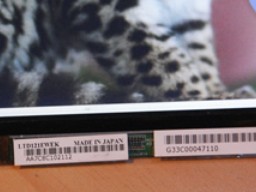
60: 54 44 31 32 31 45 57 45 4b 0a 20 20 00 00 00 ff TD121EWEK? ....
70: 00 41 41 37 43 38 43 31 30 32 31 31 32 0a 00 0d .AA7C8C102112?.?
80: 00 ff ff ff ff ff ff 00 30 64 00 56 01 01 01 01 ........0d.V????
90: 0b 12 01 03 80 1a 10 78 0a 0f 15 9a 56 4b 8b 26 ???????x????VK?&
a0: 20 50 54 00 00 00 81 00 01 01 01 01 01 01 01 01 PT...?.????????
b0: 01 01 01 01 01 01 64 19 00 36 50 20 0c 30 10 10 ??????d?.6P ?0??
c0: 62 00 05 a3 10 00 00 18 ed 10 00 36 50 20 0c 30 b.???..???.6P ?0
d0: 10 10 62 00 05 a3 10 00 00 00 00 00 00 fc 00 4c ??b.???......?.L
e0: 54 44 31 32 31 45 57 45 4b 0a 20 20 00 00 00 ff TD121EWEK? ....
f0: 00 41 41 37 43 38 43 31 30 32 31 31 32 0a 00 0d .AA7C8C102112?.?
Reverse Engineering LCD Panels
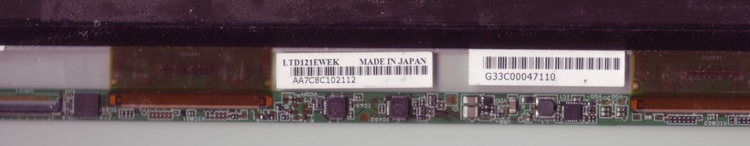
 Figure 1. PCB with LVDS pairs
DISCLAIMER: Reverse-engineering is tricky buisiness. You may permanently damage either your panel or laptop, so don’t do it on anything important! You are responsible for your own safety.
If you don’t have a datsheet for your LCD panel, it is still possible to re-use it with some reverse-engineering skills. This is easiest if you have the LCD connected to a working laptop so you can probe the signals.
I won’t do a full guide into reverse engineering here, but here are some basic tips:
Basic pin-out
First you need to locate the power supply, LVDS pairs, and optionally the EDID lines.
- Ground should be easy to locate, as it is usually connected to large copper pours, the LCD frame, LVDS shields, and the connector casing.
- V+ should have the thickest tracks on the PCB, and measure a common voltage such as 2.5, 3.3, or 5.0V. Verify this with a multimeter
- EDID should consist of 3 wires: SDA, SCL, and V_EDID. SDA/SCL will be pulled high to V_EDID, so you should find 3 pins at a common voltage. You can verify that they are EDID by using an oscilloscope and checking for data when you boot the laptop.
- The LVDS wires should also be easy to locate - they are always routed as pairs on the PCB, and the wires may be twisted or shielded. For a laptop LCD there should be 3-4 pairs.
- The backlight may or may not be on the same connector as the data. For LED screens, look for high voltages (>12V)
Backlight
There are two main types of backlighting in LCD panels: CCFL (Flurorescent), and LED. CCFL was widely used in older laptops before LED backlights came around, and are pretty obvious because you will find a large inverter module with a transformer on it, probably covered in “Warning: High Voltage!” stickers. These transformers usually have multiple pins: +V, GND, and Enable/Dimming pins. +V is usually either +12V or +5V.
LED backlights result in much thinner displays, and usually need a dedicated driver, which may or may not be built into the LCD panel. LED backlights may be split into an Anode and several Cathode wires, consiting of several “strings” of LEDs.
LVDS configuration
The LVDS configuration is trickier to figure out, but you shouldn’t need an oscilloscope (as the signals are much too fast for most low-end oscilloscopes anyway). Try disconnecting a pair from the cable and see what effect it has on the screen (refer to the data framing diagrams ):
- If you lose the picture, it is the CLK pair
- If the picture becomes scrambled horizontally, it is probably the Y2 pair (which contains HSYNC/VSYNC signals)
- If the picture gains a red or cyan tint, it is probably the Y0 pair (contians red colours)
- If the picture gains a green or purple tint, it is probably the Y1 pair (contains green colours)
Also the LVDS pairs are usually routed in order: Y0,Y1,Y2,Y3, while CLK could appear on either side.
Verifying Operation
Start by disconnecting the power supply & backlight and connecting it to your own supply (with the LVDS still connected to your laptop if possible). You should hopefully see some change in appearance of the panel.
You should be good to connect the LVDS pairs to your driver of choice, and hopefully it will get up and work. If the picture appears corrupted, you either have the polarity wrong, or have flipped Y1/Y2/Y3. If not, well I can’t really offer any advice, so you’re on your own ;)
Interfacing
If you want to use an LVDS LCD panel with a computer or SBC, you will need to find a way to interface it with your device. Since most computers/SBCs don’t have LVDS outputs, you will probably need an HDMI/DVI to LVDS converter board. Here are some options for interfacing:
-
Purchase a converter board from China (eg. Aliexpress/eBay20) Apparently you can ask the seller to match the driver board to your LCD’s datasheet, although I’ve never tried this. It should mostly just work with your panel provided it has an EDID chip.
-
Use a direct LVDS-to-HDMI converter board21 22 eg. ChalkElec’s LVDSConverter (Which is open-source !). It is very straight-forward23 - all it does is convert HDMI to TTL parallel to LVDS. There is no on-screen display or scaling involved, so whatever your computer outputs is what is displayed!
-
Parallel output to LVDS Some SBCs (eg. Beaglebone Black) will have a TTL Parallel video output, which can be converted to LVDS easily with an appropriate chip.244
-
Native LVDS output Some SBCs have native LVDS outputs (eg. RIoTBoard/SabreLITE), in which case you can simply connect the panel directly to your SBC !
In all the above cases you will need to ensure the data format of your LCD panel matches the data format of your LVDS driver. As mentioned earlier, the most common format for old LCD panels is 18bpp (3D+1C), which is compatible with a 24bpp LSB driver (since the 4th output channel Y3 can be ommitted)
Footnotes
Thanks for reading! Hopefully this guide is useful to you - if you think so, leave a comment. Knowing that people find this stuff useful gives me energy to do more experiments!
References
-
http://en.wikipedia.org/wiki/FPD-Link “Wikipedia - FPD-Link” ↩︎
-
http://www.ti.com/lit/an/snla045b/snla045b.pdf “Texas Instruments - An Introduction to FPD-Link” ↩︎
-
http://en.wikipedia.org/wiki/Low-voltage_differential_signaling “Wikipedia - LVDS” ↩︎
-
http://www.ti.com/lit/ds/symlink/sn75lvds83b.pdf “SN75LVDS83B Datasheet [pdf]” ↩︎ ↩︎ ↩︎
-
http://www.chalk-elec.com/?page_id=1284 “ChalkElec - Technical Info” ↩︎ ↩︎ ↩︎ ↩︎
-
http://www.ti.com/lit/ds/symlink/ds90c187.pdf “DSC90C187 - Low Power Dual Pixel FPD-Link Serializer” ↩︎ ↩︎ ↩︎
-
http://www.ti.com/lit/ds/symlink/ds90c3201.pdf “DS90C3201 - Dual FPD-Link Transmitter” ↩︎
-
http://en.wikipedia.org/wiki/Vertical_blanking_interval “Wikipedia - Vertical Blanking Interval” ↩︎
-
http://g3nius.org/lcd-controller/ “G3nius.org - How to control a laptop LCD panel with an FPGA” ↩︎
-
http://en.wikipedia.org/wiki/Coordinated_Video_Timings “Wikipedia - Coordinated Video Timings (CVT)” ↩︎
-
http://en.wikipedia.org/wiki/Digital_Visual_Interface “Wikipedia - DVI” ↩︎
-
http://www.cs.unc.edu/~stc/FAQs/Video/dvi_spec-V1_0.pdf “DDWG - Digital Visual Interface Specification” ↩︎
-
http://emerythacks.blogspot.co.nz/2013/04/connecting-ipad-retina-lcd-to-pc.html “EmerytHacks - Connecting an iPad retina LCD to a PC” ↩︎
-
http://hackaday.io/project/369-oscar-the-open-screen-adapter “OSCAR - The Open Screen Adapter (For iPad Displays)” ↩︎
-
http://dp2mbpr.rozsnyo.com/ “ROZSNYO - MackBook Pro Retina LCD Interface Board” ↩︎
-
https://hackaday.io/project/364-mipi-dsi-display-shieldhdmi-adapter “MIPI DSI HDMI Adapter” ↩︎
-
http://www.electricstuff.co.uk/nanohack.html “MikesElectricStuff - Ipod Nano V6 LCD hacking” ↩︎
-
http://en.wikipedia.org/wiki/Extended_display_identification_data “Wikipedia - EDID” ↩︎
-
http://msdn.microsoft.com/en-us/library/windows/hardware/jj133967%28v=vs.85%29.aspx “MSDN - Overriding Monitor EDIDs with an INF” ↩︎
-
http://www.ebay.com/sch/njytouch/m.html “NJYTouch on eBay” ↩︎
-
http://www.chalk-elec.com/?page_id=1280#!/HDMI-to-LVDS-converter/p/14647633/category=3094859 “ChalkElec - HDMI-LVDS Converter Board” ↩︎
-
http://www.raspberrypi.org/forums/viewtopic.php?f=41&t=2288&sid=3f137d035a8c1b93227525e8ee3b8761 ↩︎
-
http://www.ti.com/lit/an/slla325a/slla325a.pdf “Texas Instruments App Note - HDMI/DVI to LVDS Bridge” ↩︎
-
http://axio.ms/projects/beaglelcd/ “BeagleLCD - Beagleboard LCD Hack” ↩︎