Hackaday.IO Companion Page {resource=links}
You can get these interesting MIPI-HDMI bridge modules from China, usually with a display of some sort. They are based around the Toshiba TC358870XBG chip, which is quite a powerful beast - it can power a 4K OLED over HDMI 1.4b, or even dual 2K displays!
This makes it perfect for VR headsets, which is why you can find it in the Oculus CV1 , Razer OSVR HDK2 , HTC Vive , and the Open Source Relativ project .
This chip can also be found on these interesting MIPI-HDMI bridge modules which can be found accompanying OLED/TFT displays on AliExpress:
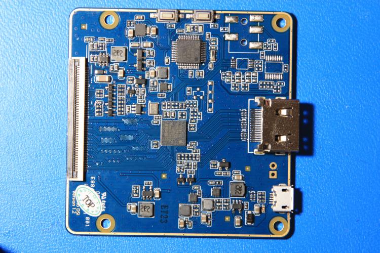
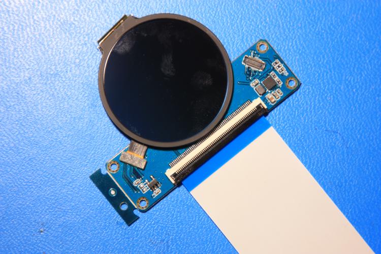
Mine came with 2x round OLED displays, presumably intended for a smart watch. The board can either duplicate the HDMI on both screens, or show independent video feeds (side-by-side).
Overview
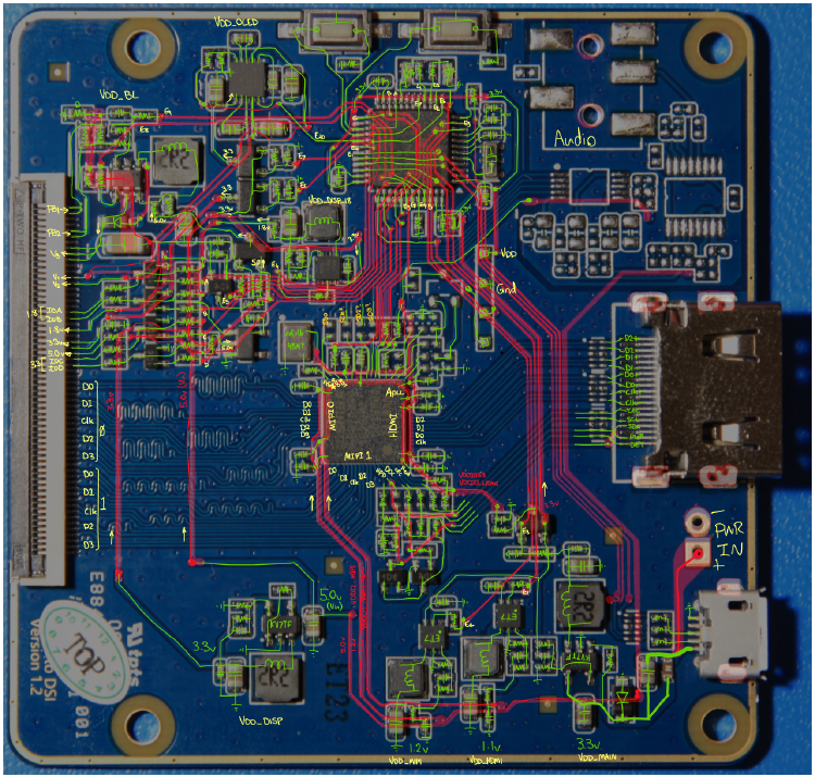
To start reverse-engineering the circuit behind this board, I started by taking photos of the bottom and top layers, and inking over with my Surface: (Click to enlarge)
 MIPI_RE
MIPI-HDMI Bridge
 ejg5qmyi
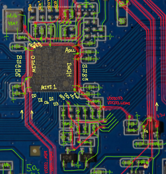
You can see that the connector on the left does indeed support two MIPI channels, each consisting of 4 data pairs & 1 clock pair. The MIPI bridge chip is connected to the MCU via I2C, and there is minimal support circuitry (only a crystal, a few buck regulators, and some passives for the PLL).
 ejg5qmyi
TODO: More details about the bridge chip
::
Power Supply
 0kkt4h0t
 ro0z5ixm
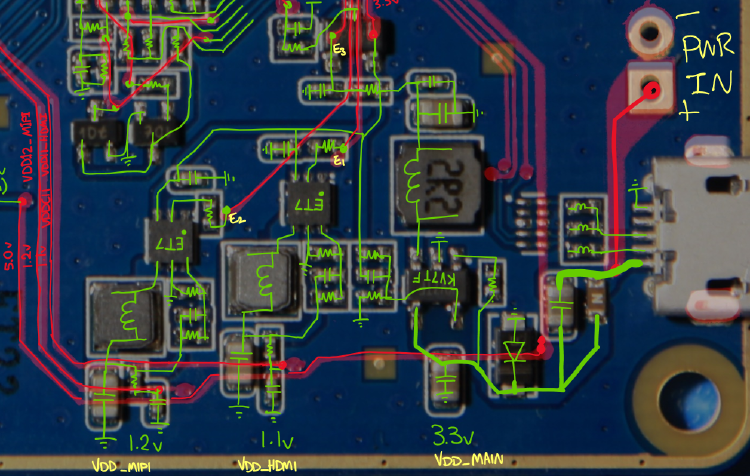
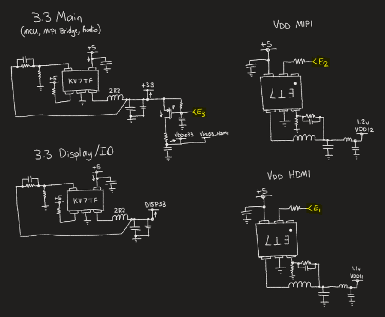
On the bottom-right you can see the main buck regulators which supply power to the MIPI bridge chip. 5.0V is fed onwards to the display buck regulators elsewhere on the PCB.
 0kkt4h0t
 ro0z5ixm
It seems the regulators behave as follows:
E1controls the 1.1v supply for the MIPI bridge (VDDC11,VDD11_HDMI)E2controls the 1.2v supply (VDD12_MIPI)E3controls the 3.3v supply for the MIPI bridge (VDDIO33,VDD33_HDMI), and the MCU & Audio circuit. I believe this defaults to on, and allows the MCU to power down the system.- The Display & IO has an always-on 3.3V supply (
DISP33)
These feed additional regulators for the OLED/TFT display…
::
MCU
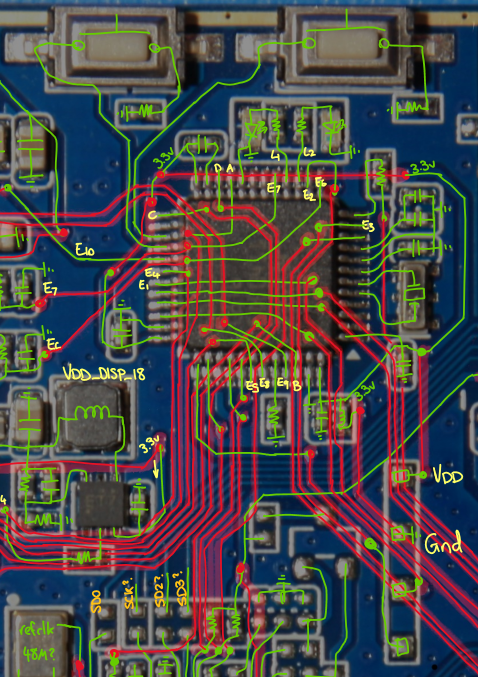 ij0e2fv8
Finally we have the GD32F103C8T6 MCU (a clone of the STM32F103) which is in charge of initalizing the MIPI chip and sequencing the power supplies
 ij0e2fv8
Those four pads on the right look interesting… could they be SWD perhaps?
(SWD Pinout: VDD, GND, PA13/SWDIO, PA14/SWCLK)
Out of curiousity, I connected an STLink to the SWD pads on the PCB, and behold, the chip is unlocked!
I was able to dump the firmware starting at 0x0800_0000, but haven’t yet gotten around to
properly reverse-engineering it.
I will revisit the firwmare in a later post…
TODO: GPIO pin map
::
Display Interface
 ym1zz8my
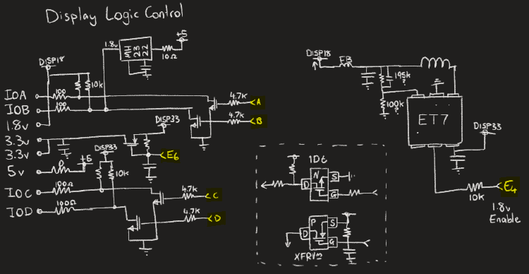
The connector provides two independent MIPI channels, each with 4 data pairs & 1 clock pair. The 5V rail is always powered, but the other rails can be individually sequenced and controlled by the MCU. The GPIOs can be used to control additional regulators or enable control signals on the display board. They are output only.
 rydd9l6b
I do not know what chip ET7 and MH 23 22 are, but they are obviously some kind of buck regulator.
I have been able to piece together the operation of this circuit, and it seems that:
A/B/C/Dare the GPIO control signals from the MCU (output only).E6enables the 3.3v rail, and supplies the 1.8v regulator.IOC/IODare powered even if this rail is not.E4enables the 1.8v rail to the display connector, but only ifE6is also enabled (for 3.3v).IOA/IOBare pulled-up to 1.8v if this is enabled.- The 5V rail is always powered.
I am not sure what the deal is with the chip at the top that is fed directly from +5v.
TODO: Full connector pinout
OLED Supplies
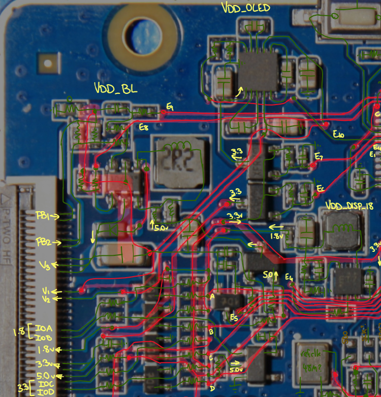 hlsohfm4
On the upper-left you can see that things get a bit more complicated. A lot of this is to support many different kinds of displays, so it provides various voltages for backlighting, OLED biasing, etc. It also supples two sets of digital outputs, one at 1.8V, and one at 3.3V.
 hlsohfm4
::
TFT Backlight Driver
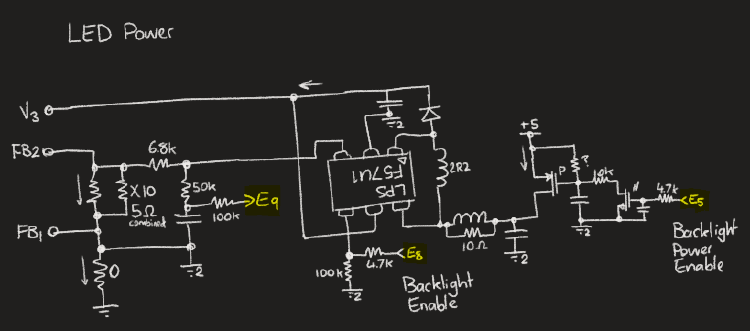
For TFTs, there is a dedicated backlight driver:
 m9g2wspn
V3is +V for the backlight, and eitherFB1/FB2can probably be chosen for -V depending on the drive strength that is desired.E9is obviously an analog feedback signal to the MCU for controlling the drive current,E5is the main supply enable, andE8is probably a PWM control signal for defining the drive current.
OLED Bias
 q5thvbbf
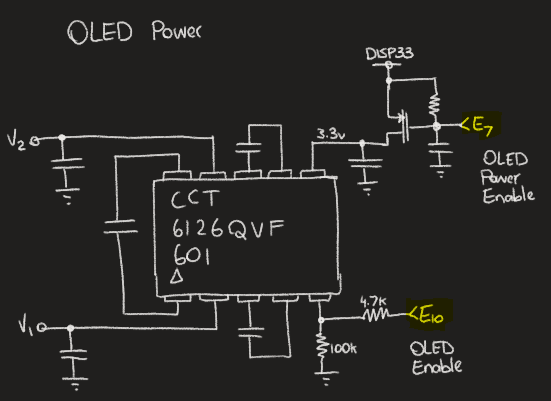
The 6126QVF is an OLED dual-rail charge pump, and looks like it can take a PWM signal to control the display brightness (since OLEDs don’t have a backlight!)
E7enables the bias circuit.E10is probably a PWM drive signal for controlling display brightness.
::
Power Sequencing
On my board, the following signals come up in this order when it is powered on:
TODO: Table
You can see that on my board, the LED backlight & OLED bias supplies are never turned on. Instead the display board has it’s own regulators which are controlled by the IOA/B/C/D GPIOs.
Breakout Board
 942481572329050865
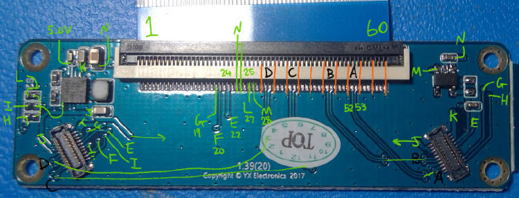
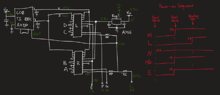
My unit came with a breakout board that supports 2x round OLED displays as mentioned above. It doesn’t actually make use of the on-board OLED charge-pump, and instead has its own regulators which are enabled via the IOA/B/C/D control signals:
 8091951572329016488
The letters signify connected net names, which helped me to map them back to the signals on the main board and work out a pinout for the OLEDs that I have:
| Pinout |
|---|
4.6V | -2.5V
4.6V | -2.5V
 GND | VDD (2.8V)
  MIPI_D | VDDIO (1.8V)
MIPI_CLK | -
TODO: Summary
I hope to further unlock the mysteries of this board, particularly on how to configure it to work with any abitrary display, and utilize the MIPI-HDMI bridge chip in my own designs…
Please leave a comment if you found this useful!
